
What is VLSI? Breaking Down Complex Chip Design Simply
Have you ever marveled at the sheer processing power packed into your smartphone, the lightning-fast calculations of your laptop, or the intricate dance of data within a supercomputer? That’s VLSI or Very Large Scale Integration, folks.
“From the smallest smart sensor in an agricultural field to the sophisticated electronics guiding ISRO's satellite launches, VLSI is the silent architect behind India's technological progress.”
Think of VLSI like a city in a chip. Just as a city has roads, buildings, utilities, and people, a VLSI chip has circuits, memory units, processors, and communication paths, engineered with precision to fit on a piece of silicon the size of a fingernail.
This article will work on demystifying VLSI, which will further open the way to the large pool of technologies intertwined by VLSI in our everyday lives.
What do you mean by VLSI?
VLSI (Very-Large-Scale Integration) refers to the process of integrating thousands to millions of transistors onto a single chip to create complex electronic circuits. It is a key technology used to design microprocessors, memory chips, and other integrated circuits that power modern electronic devices.
Why has VLSI become essential in modern electronics?
We can trace the electronics industry's remarkable growth to advances in large-scale integration technologies. VLSI technology stands out because of several key factors:
VLSI made unprecedented miniaturization possible while increasing functionality. Devices became smaller yet more powerful, creating entirely new product categories.
The integration of complete systems on single chips drastically reduced power consumption. Eliminating many interconnections between separate components also improved reliability.
This progress means we now have smartphones, high-performance computing systems, and complex telecommunications networks. Thanks to VLSI technology, our portable devices offer unprecedented processing power and application access.
How does VLSI work?
The complex process of creating a VLSI chip follows a step-by-step approach that changes abstract concepts into physical silicon implementations. A look at this process shows the complexity behind modern integrated circuits and explains how billions of transistors work together.
VLSI design flow
VLSI design flow is a structured method that helps designers create integrated circuits. This systematic approach starts with conceptualization and ends with fabrication through several distinct stages.
From specification to fabrication
The path from concept to physical chip moves through several key phases. Physical design begins after synthesis with floor planning, placement, and routing. Floor planning determines where each block in the IC layout will go and how big it should be. The team then assigns exact locations for cells on the chip to optimize performance, power, and area.
After placement, clock tree synthesis creates an efficient clock distribution network. Routing then connects all the placed cells. Design rule checks happen during this process to ensure the layout meets manufacturing specifications.
The final design moves to tape-out after physical design verification, where design data goes to the fabrication facility. The fabrication process involves several detailed steps:
- Silicon wafer preparation and cleaning
- Photolithography to transfer mask patterns
- Etching to remove unwanted material
- Deposition of new materials
- Doping to alter electrical properties
- Metallization for interconnections
These steps create physical integrated circuits on silicon wafers that are typically 12 inches wide.
Role of simulation and verification
Verification works as quality control throughout the VLSI design flow to ensure the final product works as planned. This vital part happens at multiple stages in different ways.
Functional verification checks if the design meets its intended specifications. The team simulates its behavior with various inputs and compares outputs against expectations. This uses simulation, formal verification, and static analysis for full coverage.
The team uses simulation-based techniques as the base for functional verification. These techniques find bugs in hardware models quickly, especially early in the design process. More rigorous formal methods fill any verification gaps later.
Static Timing Analysis (STA) is another key verification step. It focuses on proving timing requirements right by finding worst-case and best-case signal delays. This ensures signals reach their destinations within the required clock cycles without timing issues.
The design process uses various verification methods:
- SystemVerilog verification
- Universal Verification Methodology (UVM)
- VHDL
- Specman (e language)
- C/C++ and Python for test frameworks
Good verification reduces time to market, ensures specification compliance, improves design resilience, and lowers design failure risks. As designs become more complex, verification evolves. New methods now use artificial intelligence and machine learning to tackle verification challenges better.
Key concepts of VLSI
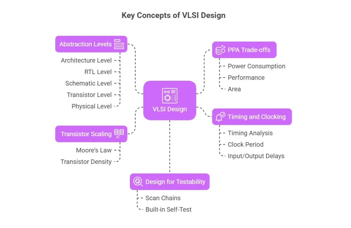
Transistor scaling and Moore's Law
Intel co-founder Gordon Moore's observation, known as Moore's Law, states that integrated circuits double their transistor count roughly every two years. The semiconductor industry has used this empirical relationship as its north star for almost 60 years. Electronic devices have seen remarkable growth due to exponential increases in transistor density. Modern chips now pack billions of transistors.
Power, performance, and area (PPA) trade-offs
PPA metrics guide all VLSI design decisions. Designers must balance these interconnected parameters to meet specific application needs. Changes to one parameter affect the others. For instance, better performance usually means higher power consumption and more area. Similarly, power optimization can expand or shrink the area based on the chosen approach. No simple formula exists for PPA optimization as each design team prioritizes different aspects based on their specific needs.
Abstraction levels in VLSI design
VLSI design uses a hierarchical approach with multiple abstraction levels:
- Architecture Level: Defines system-level functionality and sub-blocks without implementation details
- RTL Level: Describes block functionality using hardware description languages
- Schematic Level: Converts HDLs to gate-level representations using technology libraries
- Transistor Level: Implements logic gates using CMOS transistors with specific characteristics
- Physical Level: Represents the actual silicon layout ready for fabrication
- This hierarchy lets designers tackle complexity by focusing on specific aspects without drowning in lower-level details.
Importance of timing and clocking
Timing analysis is the most vital aspect of VLSI design. To prevent failures, the system needs signals to reach their destinations within specified time constraints. Proper functionality depends on the timing closure, meeting all timing requirements in various operating conditions. Static Timing Analysis (STA) checks all potential timing paths without simulation to enable thorough verification. The key timing requirements are clock period, input/output delays, and special path constraints.
Design for testability (DFT)
DFT techniques make chips easier to test by improving the observability and controllability of internal nodes. Higher chip densities have made this approach more significant. DFT features like scan chains and built-in self-test (BIST) help spot manufacturing defects accurately. These methods cut testing costs, speed up development, and boost product quality.
VLSI Tools and Applications
VLSI tools enable the design and simulation of complex microchips used in electronics. In India, they're driving innovation in sectors like consumer tech, automotive, healthcare, and defense. With rising demand and government initiatives like the India Semiconductor Mission, VLSI applications are becoming central to the nation's tech growth.
Popular EDA tools: Cadence, Synopsys, Mentor
1. Cadence: The Design Virtuoso
When you hear Virtuoso, Spectre, or Genus in an Indian VLSI lab, you know it's Cadence at work. Cadence is a mainstay in analog and mixed-signal design, areas where Indian engineers have carved a global reputation.
2. Synopsys: The Power Player of Digital Design
If you’re into RTL design, synthesis, or verification, Synopsys is your command center.
With tools like Design Compiler, PrimeTime, and VCS, Synopsys is the backbone of digital VLSI in India’s largest design houses, think Intel India, Qualcomm Hyderabad, and TCS’s semiconductor wing.
What makes Synopsys unique in India?
It’s their aggressive partnership with academia, mentorship programs for young professionals, and strong presence in the government-backed chip design initiatives like the India Semiconductor Mission (ISM).
3. Mentor (Siemens EDA): The Verification Maestro
Mentor, now part of Siemens EDA, is the go-to toolset for physical verification, layout, and PCB design, especially in automotive, aerospace, and industrial electronics.
Tools like Calibre, ModelSim, and PADS are regularly used in Indian embedded systems companies and public sector projects (hello, BEL and DRDO!).
Mentor really shines in India's tier-2 and tier-3 innovation hubs. Engineering colleges and MSMEs across Coimbatore, Nagpur, and Trivandrum are picking up Mentor tools for prototyping and verification.
Simulation and synthesis tools
SPICE (Simulation Programme with Integrated Circuit Emphasis) remains vital for circuit simulation. It accurately models electronic circuit behavior. Hardware Description Languages (HDL) like VHDL and Verilog let designers describe circuit behavior for simulation and synthesis.
Monte Carlo simulation evaluates circuit performance under manufacturing variations. Timing analysis tools find critical paths that meet timing specifications.
Applications in consumer electronics
VLSI technology has reshaped the consumer electronics scene. It powers smartphones, tablets, gaming consoles, and smartwatches. These devices use VLSI's power to blend multiple functions on small chips, reducing size and cost while improving processing capabilities.
Applications in automotive and healthcare
VLSI drives Advanced Driver Assistance Systems (ADAS), infotainment systems, and Engine Control Units (ECUs) in automotive applications. These systems enable self-driving features, object/lane detection, and live vehicle diagnostics.
Healthcare applications range from medical imaging devices to wearable health monitors and implantable medical devices. VLSI-based chips make MRI scanners, pacemakers, and glucose monitors more accurate with live monitoring capabilities.
Applications in telecommunications
VLSI technology plays a vital role in advancing telecommunications. It enables high-speed network infrastructure and 5G wireless communication. VLSI-based chips in routers, modems, base stations, and network switches ensure fast and reliable data transmission. These components support complex data processing that modern telecommunications systems need.
Career pathways in VLSI
If microchips are the brains behind modern technology, then VLSI engineers are the architects of intelligence. In this high-impact field, your career isn't just a job, it’s your chance to shape the tech that powers the world. Here's a look at the exciting paths you can take in the VLSI universe:
1. RTL Design Engineer – The Logic Builder
RTL (Register Transfer Level) designers create a chip's core functionality using languages like Verilog or VHDL. They define how data moves and processes within a chip.
2. Verification Engineer – The Design Gatekeeper
Verification engineers ensure that the chip design works as intended before fabrication. They use tools like System Verilog, UVM, and simulators to catch logical bugs early.
3. Physical Design Engineer – The Silicon Sculptor
They take the logical design and turn it into a layout ready for fabrication, handling placement, routing, timing, and power optimization.
4. DFT Engineer – The Test Strategist
Design for Test engineers insert test structures that help verify chip health after manufacturing. This ensures chips are free of defects and perform reliably.
5. Analog/Mixed-Signal Designer – The Wave Whisperer
They design circuits that handle real-world signals like sound, voltage, and RF. This is crucial for sensors, communication modules, and biomedical devices.
Essential Skills
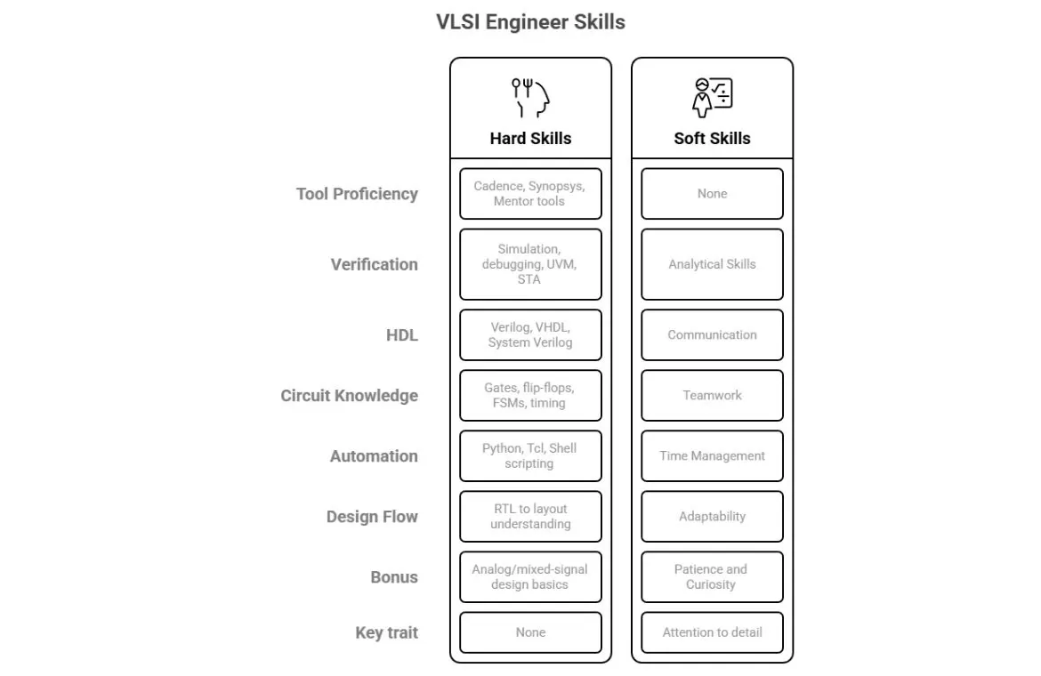
Hard Skills – The Tools of the VLSI Craftsman
- Tool Time: Get hands-on with industry-standard tools from Cadence, Synopsys, and Mentor.
- Verify Everything: Learn simulation, debugging, UVM, and static timing analysis (STA).
- Bonus Edge: Grasp the basics of analog/mixed-signal design, it’s a cherry on top. To design chips that power the future, you need a sharp technical toolkit.
- Speak Silicon's Language: Master Verilog, VHDL, and System Verilog to describe digital logic.
- Think Like a Circuit: Know your gates, flip-flops, FSMs, and timing inside out.
- Automate Like a Pro: Python, Tcl, or Shell scripting can save hours of manual work.
- Design the Full Journey: From RTL to layout, understand the entire VLSI design flow.
Soft Skills – The Silicon Behind the Scenes
A chip doesn’t work in isolation, and neither do you:
- Pixel-Perfect Precision: Tiny bugs can cost millions. Attention to detail is your superpower.
- Debug Like Sherlock: Sharp analytical skills help you find and fix the invisible errors.
- Speak Tech Clearly: Great ideas need clear communication with engineers, managers, and sometimes even clients.
- Team Player, Not Just a Coder: VLSI is a relay race, and coordination across teams is key.
- Deadlines Are Real: Learn to manage your time, especially during tape-out crunches.
- Adapt to Evolve: Tools change, technologies advance, your willingness to learn keeps you future-ready.
- Stay Patient, Stay Curious: Chip design is a marathon, not a sprint.
Both sets of skills are crucial for success in VLSI roles across design, verification, and testing.
Conclusion
At its core, VLSI is the art and science of making millions (and now billions) of transistors dance in harmony on a chip no bigger than your fingernail. Thanks to the magic of very large-scale integration, what once took rooms full of hardware can now fit in your smartwatch. It’s where design meets scale and innovation meets precision.
But understanding VLSI is not just about circuits and silicon, it's about design thinking, system-level insights, and the power to build technology that shapes the future. Whether it's the brains behind your AI assistant, the sensor in a self-driving car, or the engine of a cloud data center, VLSI is everywhere.
Breaking down VLSI is just the beginning. Building a career in it takes structured learning, hands-on practice, and mentorship from the best minds in the field. That’s exactly what the PG Level Advanced Certification Programme in VLSI Chip Design offers. Whether you're decoding RTL today or dreaming of chip-level innovation tomorrow, this program helps you turn complexity into career-defining capability.
VLSI technology works as the backbone of modern electronic systems. Your knowledge of this field helps you navigate the semiconductor industry. This applies whether you're beginning your trip or advancing your existing career. The semiconductor revolution that started decades ago continues today. VLSI innovations show no signs of slowing down.
“Because in the world of chips, your next breakthrough begins with one smart design.”
Frequently Asked Questions
Q1. What is VLSI chip design?
VLSI (Very Large Scale Integration) involves designing microchips with millions of transistors on a single chip, enabling compact, high-performance electronic systems used in smartphones, computers, and embedded devices.
Q2. What are the five levels of VLSI design?
- System Level – Defines overall system architecture and functionality.
- Register Transfer Level (RTL) – Describes data flow and control logic.
- Logic Level – Implements logic gates and circuits.
- Circuit Level – Focuses on transistor-level design.
- Layout Level – Converts circuits into a physical silicon layout.
Q3. What is RTL in chip design?
RTL stands for Register Transfer Level. It is a design abstraction used in digital circuit design to describe how data moves between registers and how the logic processes that data. RTL focuses on the flow of data, control signals, and timing, typically written using Hardware Description Languages like Verilog or VHDL. It forms the foundation for synthesizing the design into actual hardware.
About the Author
TalentSprint
TalentSprint, Part of Accenture LearnVantage, is a global leader in building deep expertise across emerging technologies, leadership, and management areas. With over 15 years of education excellence, TalentSprint designs and delivers high-impact, outcome-driven learning solutions for individuals, institutions, and enterprises. TalentSprint partners with leading enterprises and top-tier academic institutions to co-create industry-relevant learning experiences that drive measurable learning outcomes at scale.
Advance your career with the right program
Related articles

Innovation
AI Graphic Design in 2026
Design teams in 2026 aren’t short on ideas, they’re short on time. With more content to create and faster turnarounds expected, the real challenge is keeping creativity intact at scale.
AI ha

Innovation
Visual Design vs Graphic Design: Difference
In a world where every scroll, click and swipe competes for attention, design becomes the silent storyteller behind every digital moment. Yet many people confuse two

Innovation
Visual Design Principles: What Top Designers Won't Tell You
Every time you pause on a beautifully crafted website, scroll through a perfectly balanced Instagram post, or admire the elegance of a brand’s logo, you’re experiencing something deeper than good a